CHINESE
 ENGLISH
产品 >> 小金属及材料 >> 金属镓系列

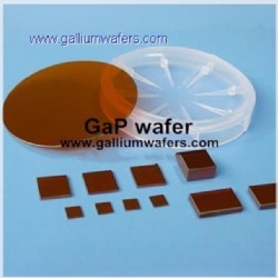
磷化镓GaP
- 型号:pmp42
Gallium Phosphide GaP wafer
Product introduction
CHINA ALLOY NEW STEVERS CO,LTD. supply GaP monocrystal materials with volume production, unique monocrystal growth control method, and the complete GaP monocrystal production line. Its products are mainly used in LED of ordinary light such as red, yellow, and green, which is as one of the primary substrates of LED.
CHINA ALLOY NEW STEVERS CO,LTD. supply GaP monocrystal materials with volume production, unique monocrystal growth control method, and the complete GaP monocrystal production line. Its products are mainly used in LED of ordinary light such as red, yellow, and green, which is as one of the primary substrates of LED.
Specifications and parameters
|
Product
|
GaP monocrystal
|
||
|
Dopant
|
S
|
Te
|
None
|
|
Carrier concentration cm-3
|
(2~7)×1017
|
(1~2)×1017
|
|
|
Mobility cm2/v.s
|
≥100
|
||
|
EPD cm-2
|
<2×10⁵
|
||
|
Diameter mm
|
50±0.5, 50.8±0.5
|
||
|
Thickness µm
|
300 ± 20
|
||
|
Crystal orientation
|
(111)±0.5°
|
||
|
Wafer surface state
|
Slice, grinding, corrosion, polishing
|
||
下一个产品:氮化镓晶片


 Mail inquiry