CHINESE
 ENGLISH
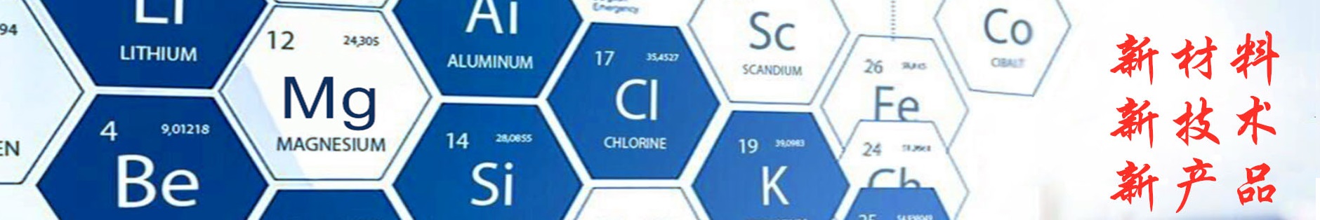
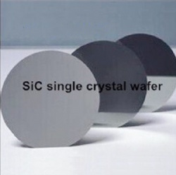
Products >> Rare metal & Wafers >> Silicon carbon SIC wafer series
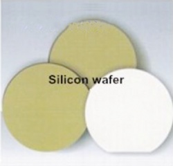
Silicon wafer
- Product No.:pmp14
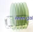
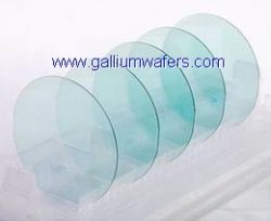
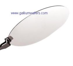
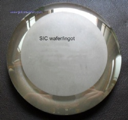
Silicon wafer /Silicon single crystal wafer
Silicon wafer used for solar cell :
Monocrystalline/Polycrystalline N type
Diameter:156mmx156mm
Thickness:200mm,
Orientention:100
Resisitivity:1-3 ohm cm
Special order is workable! Plz mail to i[email protected] for details!
Usage:used as a semiconductor material,high powder transistor,rectifier,solor cell etc.
| Major capability parameter | ||
| Crystal Structure | M3 | |
| Melt point(℃) | 1420 | |
| Density | 2.4(g/cm3) | |
| Doped material | No doped | |
| Type | P | |
| Resistivity | 10-3~40Ωcm | |
| E P D | ≤100∕cm2 | |
| O Content(∕cm3) | ≤1~1.8×10¹⁸ | |
| C Content(∕cm3) | ≤5×10¹⁶ | |
| Size |
10×3m、10×5m、10×10mm、15×15mm、20×15mm
Special size and orientation are available upon request
|
|
| Thickness | 0.5mm、1.0mm | |
| Size Tolerances | <±0.1mm | |
| Thickness Tolerances | <±0.015mmspecial in<±0.005mm) | |
| Polishing | Single or double | |
| redirection precision | ±0.5° | |
| Redirection the edge: | 2°(special in 1°) | |
| Crystal orientation | <100>、<110>、<111> | |
| Pack | 100 clean bag,1000 exactly clean bag | |
Silicon wafer used for solar cell :
Monocrystalline/Polycrystalline N type
Diameter:156mmx156mm
Thickness:200mm,
Orientention:100
Resisitivity:1-3 ohm cm
Special order is workable! Plz mail to i[email protected] for details!
Contact:Jason Wang Mobile:+86-18039202132
Previous Product:2inch SIC wafer
Next Product:SiC single crystal wafer
Products Category
Contact Us

Name: Jason Wang
Tel: +86-18039202132
E-mail: [email protected]
Add: Material Industrial Park, Science avenue, Zhengzhou, Henan, China

 Mail inquiry