CHINESE
 ENGLISH
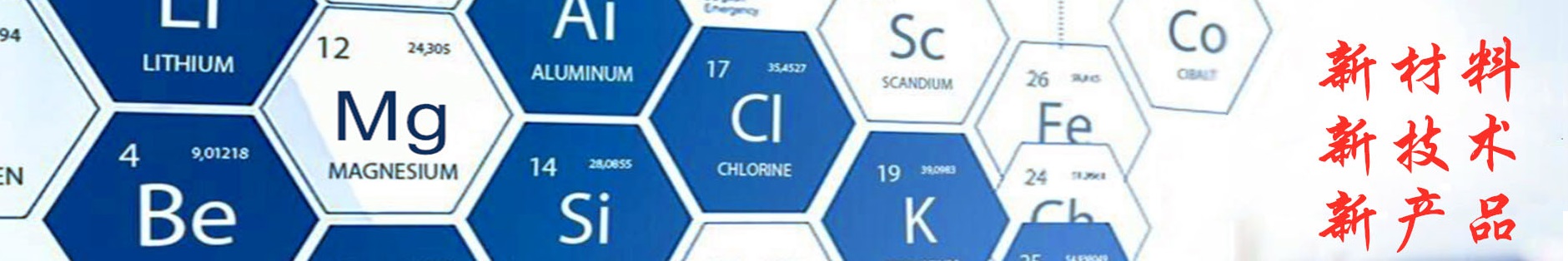
Products >> Rare metal & Wafers >> Gallium series
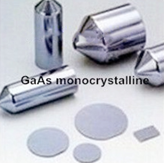
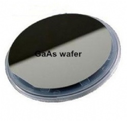
GaAs monocrystalline wafer
- Product No.:pmp4
GaAs monocrystalline
We can provide GaAs monocrystalline with different types and resistivity to meet your demands!
|
Dopant
|
Si
|
Zn
|
Si
|
|
Diameter
|
50.8±0.4
|
50.8±0.4
|
63.5±0.4
|
|
Growth method
|
VGF
|
VGF
|
VGF
|
|
Conduct Type
|
N
|
P
|
N
|
|
Orientation
|
<511>,<100>
upon request
|
<100>
upon request
|
<100>
upon request
|
|
CC (/cm3)
|
4.0E17 / 2.5E18
|
1.5E19 / 3.0E19
|
1.0E17 / 7.0E17
|
|
Mobility (cm2/v.s)
|
>2000
|
>2000
|
>2000
|
|
EPD (/cm2)
|
<3000
|
<5000
|
<8000
|
|
Primary Flat
|
EJ (0-1-1)±0.5°
|
EJ (0-1-1)±0.5°
|
EJ (0-1-1)±0.5°
|
|
PFlat Length (mm)
|
17±1
|
17±1
|
17±1
|
|
Secondary Flat
|
EJ(0-11)±0.5°
|
EJ(0-11)±0.5°
|
EJ(0-11)±0.5°
|
|
SFlat Length (mm)
|
7±1
|
7±1
|
7±1
|
|
Thickness (um)
|
295±5
upon request
|
295±5
upon request
|
295±5
upon request
|
|
Surface Front
|
polished
|
polished
|
polished
|
|
Finish Back
|
sliced & etched
|
sliced & etched
|
sliced & etched
|
|
Epi-Ready
|
Yes
|
Yes
|
Yes
|
We can provide GaAs monocrystalline with different types and resistivity to meet your demands!
Special order is workable! Plz mail to [email protected] for details!
Contact:Jason Wang Mobile:+86-18039202132
Previous Product:GaAs wafer
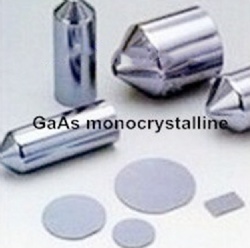
Next Product:GaAs polycrystalline
Products Category
Contact Us

Name: Jason Wang
Tel: +86-18039202132
E-mail: [email protected]
Add: Material Industrial Park, Science avenue, Zhengzhou, Henan, China

 Mail inquiry